Power Optimization Related
Additional routing increases wire congestion and power consumption. Solutions:
Adjust settings/constraints
Increase pipeline registers to shorten long paths
Power consumption of storage resources:
Force the use of small MLAB blocks, avoid using large M20K blocks, suitable for large bit-width but shallow memory
Power consumption mainly comes from dynamic clocking, charging and discharging RAM core leads to increased power consumption, reducing memory clocking events can reduce power consumption
Use clock enable signals to make memory devices achieve almost zero power consumption when not in use (no RAM core charging and discharging)
Use narrower/deeper memory implementations, control RAM depth with
max_block_depth, at this time the compiler will add extra decoder and mux logic,
Pipeline
Improve speed, shorten logical depth, reduce logical switching, without changing the original logical function
Will increase resource/register usage, affect delay and throughput, if the design has glitches, it may increase power consumption
I/O Power Consumption
Power consumption formula:

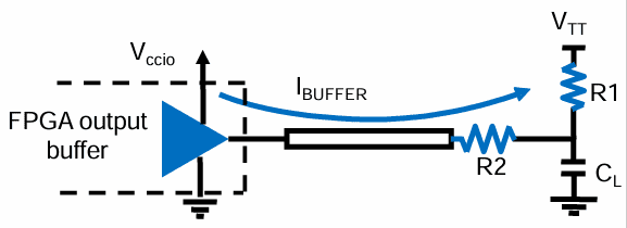
Lower I/O voltage consumes less power
Resistor pull-up standards (SSTL/HSTL): output fluctuation is small, dynamic power consumption is lower in high-frequency applications, but static power consumption is high due to continuous driving of static resistance
Non-pull-up standards (LVTTL/LVCMOS): V = Vccio, high dynamic power consumption at high frequencies, but low static power consumption due to no static resistance driving
Some Basic Syntax
Assignment:
assign out = in;Inverse assignment:
assign out = ~in;XOR:
assign out = a ^ b;XNOR:
assign out = ~(a ^ b);casez: can introduce don't-care bits in case:
always @(*) begin
casez (in[3:0])
     4'bzzz1: out = 0;   // in[3:1] can be anything
     4'bzz1z: out = 1;
     4'bz1zz: out = 2;
     4'b1zzz: out = 3;
     default: out = 0;
 endcase
 end
FPGA Design Flow:
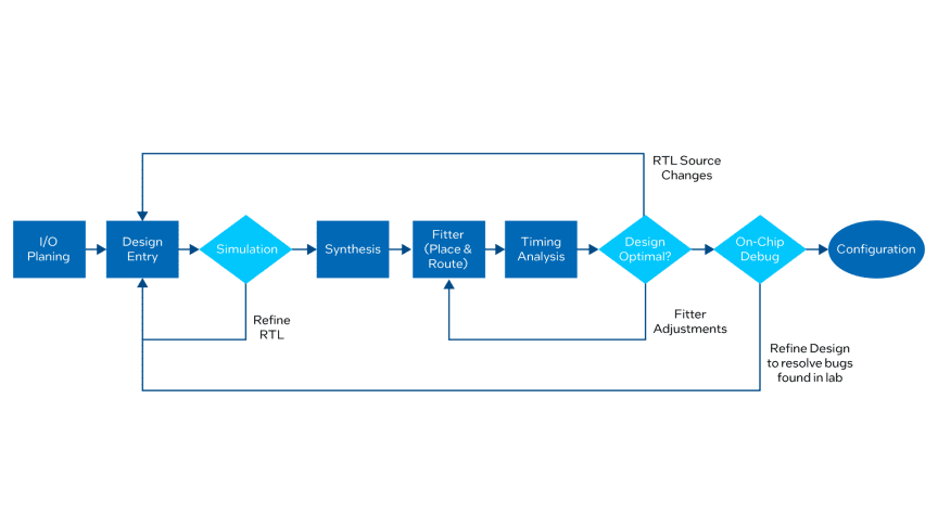 The official FPGA design flow from Intel related documentation is quite detailed and includes online learning courses.
Competition and Hazard:
Competition: In combinational logic circuits, signals pass through multiple paths to reach the output, and each path goes through different logic gates, resulting in time differences. At the moment of signal change, there is a sequence of precedence, which is called competition.
Hazard: Due to competition, unexpected signals appear in the circuit output, causing transient errors, known as hazards. This is manifested as narrow pulses, or glitches, at the output that were not originally designed.
A common method to determine if competition and hazards exist using logical algebra is to check if the output logical expression contains a "and" or "or" relationship between a signal's original variable A and its inverse variable /A, and if A and /A pass through different propagation paths. Then, competition exists. Solutions include modifying the logical expression to avoid this situation, using sampling sequential logic and only sampling at the clock edge, or using external capacitors to eliminate narrow pulses in parallel.
Causes and Elimination of Metastability
In asynchronous systems, metastability occurs when the setup and hold times of registers are not met. Typical cases include data transmission across clock domains and asynchronous reset circuits. During asynchronous transmission, metastability can be eliminated through single-bit signal dual-register synchronization and multi-bit signal FIFO bridging (in fact, asynchronous signal synchronization is a method to eliminate metastability in asynchronous transmission). Asynchronous reset and synchronous release can eliminate metastability caused by asynchronous reset.
Difference between Latch and Flip-Flop
Level-sensitive storage devices are called latches. They can be divided into high-level and low-level latches, used for signal synchronization between different clocks.
Bistable storage elements composed of cross-coupled gates are called flip-flops. They can be divided into rising edge and falling edge trigger types. A flip-flop can be considered as two different level-sensitive latches connected in series. The first latch determines the setup time of the flip-flop, and the second latch determines the hold time.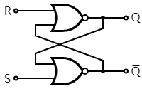 SR Latch, built using NOR gates, Set/Rest is 1 when Q is 1
 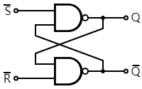 ~SR Latch, opposite of the above, built using NAND gates, input and output are opposite to SR Latch
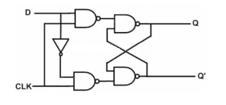 D Flip-Flop, Q follows D input on rising edge of CLK, otherwise keeps the previous value
Two Types of Storage Resources in FPGA Chips
There are two types of storage resources in FPGA chips: one is called BLOCK RAM, and the other is internal storage (also known as distributed RAM) configured by LUT. BLOCK RAM is composed of a certain number of fixed-size storage blocks. Using BLOCK RAM resources does not occupy additional logic resources and is fast. However, using BLOCK RAM resources consumes resources in integer multiples of the block size.
Iss
若无法加载请检查网络环境。
若无法加载请检查网络环境,或切回 Disqus 稍后再试。